
Wafer inspection systems generate a large amount of information: defect coordinates, wafer maps, die images, classification results, equipment status, recipe parameters, alarms, and production statistics. Although the inspection sensor and analysis software determine whether a defect can be detected, the LCD display determines how effectively operators and process engineers can understand and act on that information.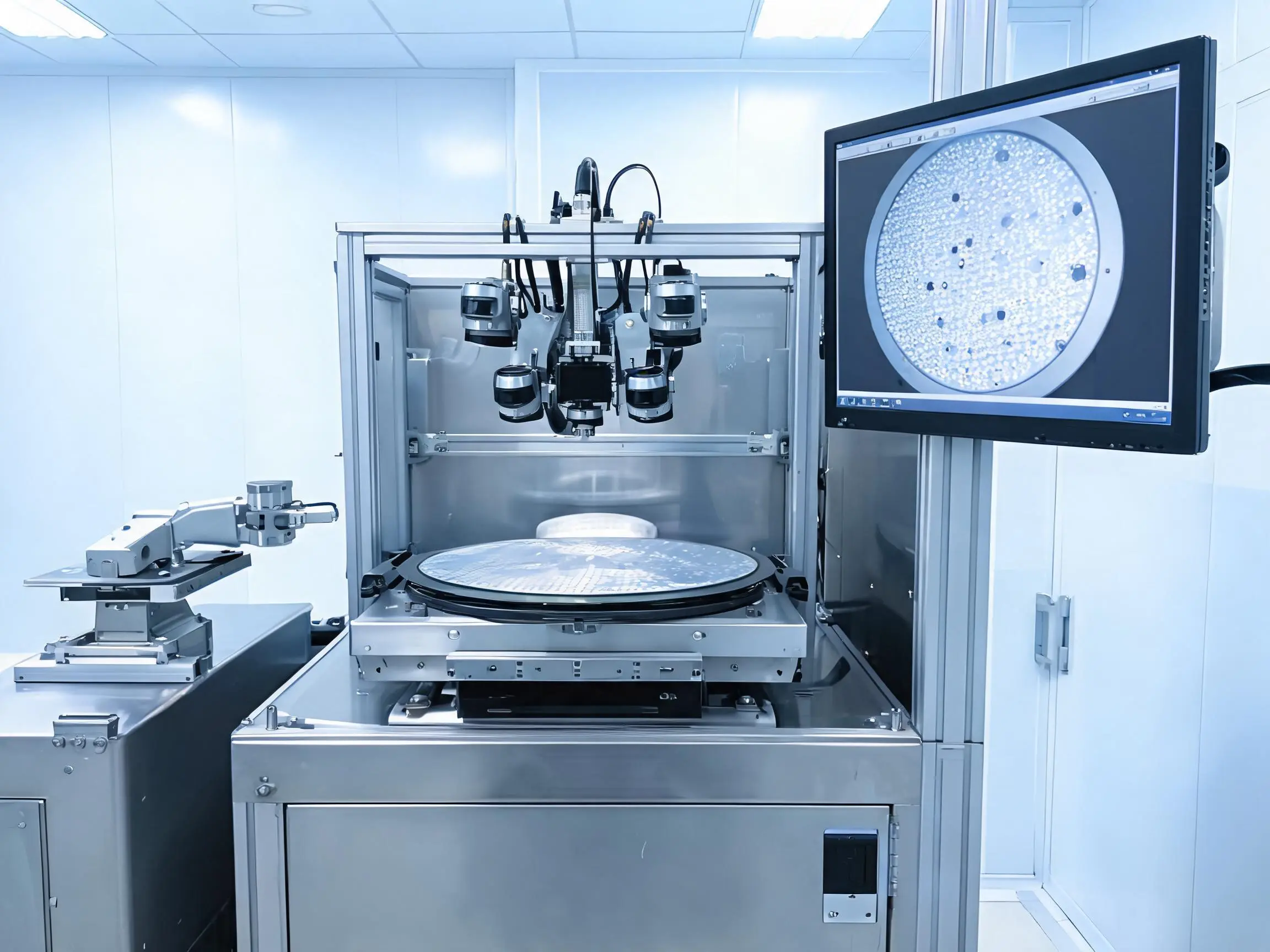
In semiconductor production, this distinction matters. A display does not improve the optical sensitivity of a dark-field inspection system or the resolution of an electron-beam review tool. What it can improve is the speed and consistency of defect review, equipment operation, alarm response, recipe verification, and maintenance diagnosis.
From my experience working with industrial LCD projects, wafer inspection equipment places unusually high demands on information density and visual consistency. A screen may need to present a complete wafer map while simultaneously showing defect images, coordinates, classification data, and tool status. If the resolution is inadequate, the interface is poorly scaled, or the touchscreen produces unintended inputs, the inspection system becomes harder to operate even when the underlying detection technology performs correctly.
Quick Answer: LCD displays improve wafer inspection systems by presenting wafer maps, defect images, inspection results, equipment status, and control functions in a clear and organized interface. A properly selected industrial LCD helps operators locate defects, compare inspection images, review exceptions, respond to alarms, and manage the equipment efficiently. Important selection factors include resolution, viewing angle, contrast, surface reflection, touch performance, interface compatibility, mechanical integration, reliability, and long-term availability.
The correct display specification depends on how the inspection tool will be used. A local equipment HMI, an engineering review station, and a maintenance panel may all require different screen sizes, resolutions, touch technologies, and optical characteristics. The display should therefore be selected around the actual workflow rather than treated as a generic computer monitor.
Claim: In a wafer inspection system, the LCD is not the defect-detection device. Its value lies in turning complex inspection and equipment data into information that operators and engineers can review, interpret, and act on accurately.
1. What Information Do LCD Displays Present in Wafer Inspection Systems?
A wafer inspection tool rarely presents only a live image. Its user interface combines information from the inspection module, wafer handling system, motion platform, image-processing software, recipe database, factory host, and equipment diagnostics. The LCD must organize these data without forcing the operator to move repeatedly between disconnected screens.
Wafer Maps and Defect Coordinates
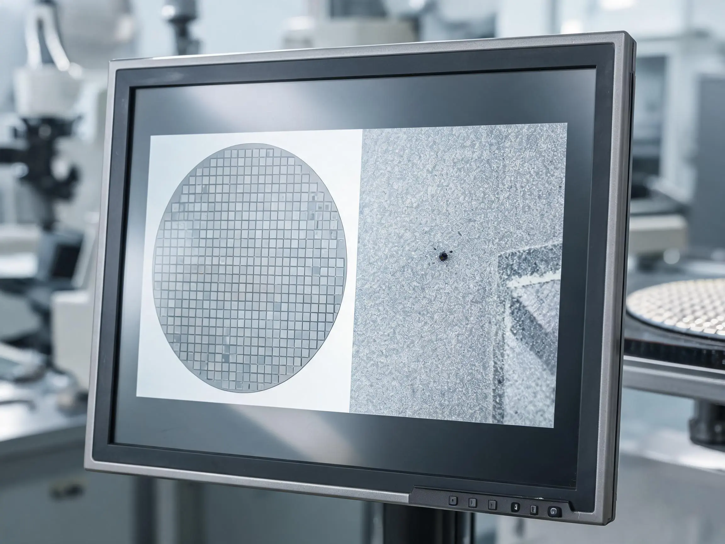
The wafer map is one of the most recognizable elements of an inspection interface. It shows the position of dies or inspection zones and marks detected defects according to location, type, severity, or review status. Operators can use the map to identify clusters, edge-related patterns, repeating defects, scratches, particles, or process signatures distributed across the wafer.
When the screen resolution is too low, small map markers become difficult to separate and coordinate labels may overlap. This does not change the inspection result stored by the software, but it makes visual analysis slower. A higher-resolution display allows the interface to show the overall wafer distribution while preserving enough detail for the operator to select individual defect locations.
Defect Images and Comparison Views
Inspection and review systems may display bright-field images, dark-field responses, differential images, scanning electron microscope images, or processed defect thumbnails. Depending on the equipment, the interface may provide side-by-side views of a detected defect and a reference area. It may also show different magnifications, image channels, or previous inspection results.
These images help an engineer determine whether an event is a particle, pattern anomaly, scratch, residue, nuisance signal, or another defect category. For this task, resolution and grayscale separation are generally more important than excessive brightness. Color may be used for overlays, classification labels, heat maps, and status indicators even when the source inspection image is monochrome.
Classification and Statistical Information
Modern inspection platforms can automatically classify many detected events, but engineers still need to review exceptions and understand how the results are distributed. The LCD may present defect counts, classification tables, histograms, Pareto charts, trend data, confidence levels, and lot-to-lot comparisons.
Information density should be handled carefully. Placing every available measurement on one screen can make the interface harder to read. In well-designed equipment, the display first presents the information needed for the current task and then allows the user to open more detailed views.
Equipment and Process Status
The screen may also show wafer and carrier identification, inspection recipe, scan progress, stage position, robot status, vacuum condition, sensor health, throughput, communication status, and active alarms. These items are operational rather than analytical, but they are essential to safe and efficient production.
Clear separation between inspection results and machine status reduces mistakes. For example, an operator should be able to distinguish a process-related defect warning from an equipment fault that requires the inspection cycle to stop.
Claim: The display in a wafer inspection system must present both defect information and equipment status. Its effectiveness depends on how clearly it organizes wafer maps, images, classification results, recipe data, and machine conditions within the operator’s normal workflow.
2. How Do LCD Displays Improve Inspection and Review Workflows?
The main operational benefit of a well-integrated display is not simply that it shows more data. It reduces the number of steps required to move from inspection to understanding and from understanding to action.
Faster Navigation from Wafer Map to Defect Detail
A practical review workflow often begins with the overall wafer map. The operator selects a region or defect marker, opens the corresponding image, checks its coordinates and classification, compares it with reference data, and then accepts, changes, or escalates the classification.
A display with sufficient resolution can keep the wafer map, image viewer, and essential defect data visible at the same time. This reduces repeated window switching. The benefit becomes more noticeable when an engineer must review hundreds of exceptions during recipe development or process troubleshooting.
Clearer Alarm Recognition and Response
Inspection equipment combines subsystems with different failure modes. A wafer-handling error, stage-position fault, illumination problem, communication interruption, or thermal warning requires a different response. The HMI should communicate the alarm source, severity, affected module, and permitted next action clearly.
Display readability is especially important when the operator is not standing directly in front of the machine. Wide viewing angles, suitable character sizes, consistent status colors, and controlled reflections help personnel recognize abnormal conditions from different positions around the tool.
More Efficient Touch-Based Operation
A touchscreen can simplify job selection, wafer map navigation, image zooming, alarm acknowledgement, and maintenance menus. It also reduces the need for an exposed keyboard and mouse near the equipment. However, touch control must be designed for deliberate operation rather than added only for convenience.
Small controls, crowded menus, and gesture-dependent actions can become unreliable when operators wear gloves. Critical commands should require clear confirmation, and functions such as emergency stopping must remain part of the equipment’s dedicated safety circuit. A touchscreen must never replace physical interlocks or emergency controls.
For a broader discussion of touch interfaces in advanced equipment, see How Do Touchscreens Improve AI Equipment Management?. The application is different, but many principles involving glove operation, interface layout, accidental-input prevention, and maintenance access also apply to semiconductor equipment.
Better Support for Engineering and Maintenance
Production operators usually need a controlled set of functions. Process engineers and service technicians need more detailed access to calibration values, subsystem states, communication logs, image settings, sensor diagnostics, and historical alarms.
A suitable LCD allows the software to organize these functions into role-based views. The production screen remains simple, while engineering and service pages can display denser technical information. This approach improves usability without hiding diagnostic data from qualified personnel.
Reduced Risk of Operational Misinterpretation
Poor display performance can create subtle problems. Reflections may obscure a warning. Incorrect scaling may make text or markers appear soft. Weak grayscale differentiation may hide details in a review image. An unstable touch panel may select the wrong control. None of these issues changes the raw inspection data, but each one can affect how a person responds to it.
In high-value semiconductor production, small operational delays and incorrect decisions can have large consequences. The display should therefore be evaluated as part of the equipment’s human-machine interface, not as a replaceable office accessory.
Claim: A properly designed LCD interface shortens the path from defect detection to review, classification, alarm response, and maintenance action. The improvement comes from better access to information and more reliable interaction—not from altering the inspection sensor’s detection capability.
3. Which Display Specifications Matter Most for Wafer Inspection?
Display selection should begin with the software layout and operator workflow. Choosing a panel according to diagonal size alone is one of the most common mistakes in equipment development.
Screen Size, Resolution, and Pixel Density
Compact local control panels may use a 10.1-inch, 12.1-inch, or 15.6-inch LCD. Larger inspection and review interfaces often require 17-inch, 18.5-inch, 21.5-inch, 23.8-inch, or larger displays. The correct size depends on the installation space, viewing distance, software layout, and amount of information displayed simultaneously.
Resolution is often more important than physical size. A large screen with inadequate resolution does not automatically show more useful information. Wafer maps, defect thumbnails, fine text, tables, and image viewers benefit from Full HD or higher resolution when the host computer and application software support it.
Scaling must also be tested. Some legacy semiconductor applications were created for a fixed resolution and may not scale correctly on a high-pixel-density panel. Labels can become too small, controls can move outside the visible area, or graphical elements can be interpolated incorrectly. The proposed display should be tested with the actual user interface rather than only with standard desktop images.
For additional guidance on matching display dimensions to equipment interfaces, refer to What Display Sizes Are Common in AI Equipment?. Although semiconductor machines have different layouts, the same engineering relationship between viewing distance, information density, enclosure space, and resolution remains relevant.
Contrast, Grayscale, and Color Consistency
Inspection images can contain subtle differences in brightness and texture. A display with stable contrast and good grayscale separation makes these differences easier to review. Wide viewing technology such as IPS-type LCD construction is often preferred when several people may view the display or when the operator cannot remain directly in front of it.
Color consistency matters for interfaces that use heat maps, overlays, classification colors, and status indicators. However, the required level of calibration depends on the role of the screen. If the local HMI is primarily used for equipment operation and process observation, normal industrial color stability may be sufficient. If engineers use the screen for final visual defect judgment, the display, graphics path, software rendering, and calibration procedure must be evaluated as one system.
A high-specification panel alone does not create a metrology-grade viewing station. Graphics processing, video conversion, gamma settings, operating-system color management, ambient lighting, and panel aging can all influence the displayed result.
Brightness and Surface Reflection
Wafer inspection equipment is normally used indoors, so extreme outdoor brightness is rarely necessary. In many cleanroom and laboratory environments, approximately 300 to 500 nits can provide comfortable visibility, depending on the cover glass, lighting, viewing distance, and enclosure design.
Reflection control may be more valuable than simply increasing luminance. Overhead lighting can produce visible reflections on untreated glass, particularly when dark inspection images are displayed. Anti-glare or anti-reflective surface treatments can improve readability, but they should be tested with the actual image content. Heavy matte treatment may reduce reflections while also making fine image details appear slightly less sharp.
Touchscreen Technology
Projected capacitive touchscreens provide a modern interface, good optical clarity, and multi-touch capability. They are suitable when glove requirements, grounding, electromagnetic noise, and cover-glass thickness are understood during development.
Resistive touchscreens remain practical for applications requiring reliable operation with thick gloves, styluses, or nonconductive objects. They do not provide the same optical appearance or gesture performance as projected capacitive touch, but they can be a sensible choice for maintenance terminals or equipment based on an established interface design.
For projected capacitive touch, the touch controller firmware must be tuned around the final cover glass, bonding structure, enclosure grounding, cable routing, and noise environment. A touchscreen that operates correctly as an open sample may behave differently after installation beside motors, switching power supplies, illumination drivers, and high-speed electronics.
Temperature, Backlight Life, and Continuous Operation
The ambient cleanroom temperature may be controlled, but the temperature inside the display enclosure can be considerably higher. Heat generated by the host computer, power supply, controller board, and backlight can accumulate behind a flush-mounted screen.
The panel should be selected according to the measured internal temperature, expected duty cycle, and ventilation design. For continuously operating equipment, backlight life, brightness decay, image retention behavior, and thermal stability deserve particular attention.
The reliability principles discussed in Why Is Reliability Important for AI Server Displays? also apply here: the display must remain available when operators need diagnostic and control information, particularly during abnormal equipment conditions.
Interface and Product Availability
Industrial panels may use LVDS or eDP, while complete monitor assemblies commonly use HDMI or DisplayPort. Touch interfaces may use USB or I2C. The choice should match the host architecture, cable distance, available connectors, boot behavior, and service strategy.
Long-term availability is especially important because semiconductor tools can remain in production for many years. Replacing a discontinued panel may require changes to the mounting structure, display controller, cable, touch firmware, optical bonding, and software scaling. A controlled industrial display platform can reduce this redesign risk.
Different industrial LCD architectures and integration options are explained further in Which Industrial LCD Solutions Support AI Infrastructure?. Many of the same options—open-cell panels, TFT LCD modules, touch assemblies, and complete display units—are used when configuring semiconductor equipment interfaces.
Claim: The best wafer inspection display is not necessarily the brightest or largest panel. It is the display whose resolution, optical performance, touch behavior, interface, operating life, and mechanical format match the actual inspection software and equipment environment.
4. How Should Wafer Inspection Displays Be Integrated and Validated?
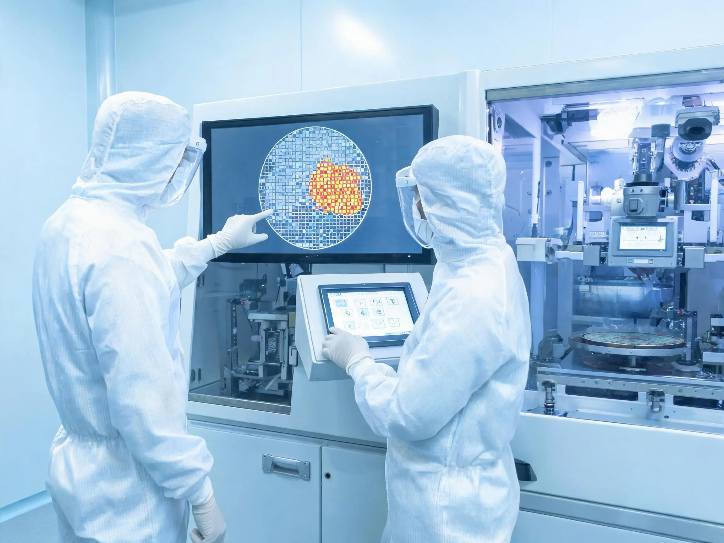
A suitable LCD specification is only the starting point. The final performance depends heavily on the cover glass, bonding, enclosure, controller board, cable design, grounding, software, and thermal conditions.
Design the Display Around the Final Equipment Structure
Wafer inspection displays are often installed behind a flush front surface so that the equipment is easier to operate and clean. Custom cover glass can provide the required outer dimensions, printed border, logo, touch area, mounting features, and surface treatment.
The cover glass and enclosure should minimize ledges and gaps where contamination can collect. Sealing requirements must be defined at the equipment level. An LCD panel by itself should not be described as cleanroom-ready or ingress-protected; these characteristics depend on the completed mechanical assembly.
Cleaning materials must also be considered. The glass coating, printing, adhesive, gasket, and touch structure should be compatible with the cleaning procedure planned for the equipment. Repeated wiping can damage an unsuitable surface treatment even when the LCD beneath it continues to operate normally.
Evaluate Optical Bonding Where It Provides Real Value
Optical bonding removes the air gap between the LCD and cover glass or touchscreen. It can reduce internal reflections, improve perceived contrast, strengthen the front assembly, and prevent dust from entering the viewing gap.
These advantages can be useful for inspection equipment, particularly when dark images are displayed under bright overhead lighting. Nevertheless, bonding adds cost and affects repair strategy. The benefits should be evaluated against screen size, optical requirements, serviceability, expected production volume, and the replacement plan for the bonded assembly.
Confirm Video Timing and Software Compatibility
The actual equipment computer should be used during validation. Engineers should confirm native resolution, refresh rate, scaling, color format, startup timing, sleep recovery, cable length, and behavior after unexpected power interruption.
Inspection applications deserve special attention because some use fixed window dimensions or specialized graphics rendering. Test the complete workflow: recipe selection, wafer-map display, image review, defect-marker selection, alarm pages, maintenance menus, and report views. A panel that displays a desktop correctly may still reveal scaling problems inside the inspection application.
Validate Touch Performance in the Installed Condition
Touch testing should use the intended gloves and the final cover-glass structure. It should include taps near the edge, dragging across a wafer map, image zooming, long presses, rapid repeated inputs, and operation while other equipment modules are active.
False touches and loss of sensitivity can result from poor grounding, electrical noise, liquid on the glass, an unsuitable controller configuration, or excessive cover-glass thickness. These issues are easier to solve before the equipment enters formal qualification.
Test Thermal, EMC, ESD, and Mechanical Performance
The display should be operated inside the final or representative enclosure while temperatures are measured at critical points. Testing should cover maximum brightness, continuous operation, system startup, and the highest expected internal load.
Electromagnetic compatibility and electrostatic discharge testing must include the final cables, grounding method, touch controller, display controller, power supply, and enclosure. Vibration and mechanical testing should confirm that mounting pressure does not distort the panel or create bright spots.
Validation should also include repeated cleaning, connector cycling where relevant, power cycling, backlight adjustment, and recovery from communication faults. For equipment expected to operate for many years, it is wise to record the approved panel revision, controller firmware, cable specification, touch parameters, and optical stack.
Plan for Replacement Before Production Begins
A replacement strategy should define whether the service item is the bare LCD, the touch-display assembly, or a complete monitor module. If the original panel becomes unavailable, an approved alternative should be evaluated for mechanical dimensions, active area, brightness, color, viewing angle, power, video timing, connector position, touch response, and software compatibility.
Substitution based only on diagonal size and resolution is risky. Two panels with the same nominal specification may differ in outline dimensions, mounting points, cable position, timing requirements, and optical appearance.
Claim: Wafer inspection display validation must cover the complete installed assembly. Mechanical design, optical bonding, software scaling, touch tuning, grounding, thermal conditions, EMC, cleaning, and replacement planning can be as important as the LCD panel specification itself.
5. What Advantages Does XIANHENG Offer for Wafer Inspection Display Projects?
XIANHENG supports industrial display projects from initial panel selection through touchscreen, cover-glass, bonding, cable, controller, and complete display integration. For wafer inspection equipment, this makes it possible to evaluate the display as a working HMI assembly rather than as an isolated panel.
Industrial LCD Selection from Established Manufacturers
We can support LCD options from manufacturers such as BOE, AUO, Innolux, and Tianma. Available solutions include compact control-panel displays, Full HD operator screens, high-resolution panels, wide-viewing-angle LCDs, high-brightness versions, and models designed for extended operating temperatures.
Panel selection can be based on the equipment software, installation dimensions, interface, thermal environment, viewing distance, availability expectations, and target production period. Customers can review suitable options through the Industrial LCD Product Collection.
Touchscreen and Cover-Glass Customization
XIANHENG can provide projected capacitive or resistive touch solutions according to the required operating method. Custom cover glass can include specified dimensions, thickness, printed borders, logos, transparent windows, surface treatments, and mechanical features.
For projected capacitive touch projects, we can work with customers on cover-glass structure, glove operation, interface selection, controller tuning, cable layout, and compatibility with the final enclosure.
Optical Bonding and Display Assembly Support
Optical bonding is available for projects that require lower reflection, improved perceived contrast, or a sealed optical stack. XIANHENG can also support customized display cables, adapter boards, controller boards, and integrated touch-display assemblies.
This reduces the number of separate components the equipment manufacturer must coordinate and provides a clearer specification for production and after-sales replacement.
OEM and ODM Engineering Cooperation
During the early project stage, our engineering team can review the required size, resolution, brightness, interface, operating temperature, touch method, cover-glass design, bonding requirement, cable arrangement, and expected product life.
Samples can then be prepared for software, optical, touch, mechanical, thermal, and electrical testing. The same development approach described in How Can XIANHENG Support AI Hardware Manufacturers? can also be applied to semiconductor inspection equipment, with validation adapted to cleanroom use, defect-review interfaces, and long equipment lifecycles.
Lifecycle and Replacement Planning
For semiconductor equipment, display continuity should be considered before volume production. XIANHENG can help customers compare industrial panel options, define critical specifications, evaluate alternatives, and develop a more manageable replacement path if the original model approaches end of life.
To discuss a wafer inspection display, touchscreen, optical bonding, or customized HMI assembly, please reach out to XIANHENG with the required screen size, resolution, interface, touch method, operating environment, annual demand, and available mechanical drawings.
Claim: XIANHENG combines industrial LCD sourcing with touchscreen, cover-glass, optical-bonding, controller, cable, customization, and lifecycle support, helping wafer inspection equipment manufacturers develop display assemblies around their actual mechanical and operational requirements.


